產品介紹
-
-
矽光子元件
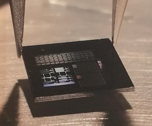
產品說明
Overview of the NanoSOI Silicon Photonics fabrication service.
| Rapid fabrication service for prototyping silicon photonic integrated circuits. Includes passive and thermo-optic devices. | |
| Turnaround time from design submission to delivery as short as three weeks. | |
| Options for cladding oxide, metallization and deep trenches for edge-coupling. | |
| Proven optical performance and low propagation loss. |
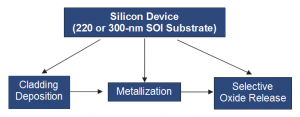
The NanoSOI fabrication process provides an avenue to fabricate photonic integrated circuits (PICs) as well as micro-electromechanical systems (MEMS). The foundation of the process is the silicon patterning step, which is performed on silicon-on-insulator (SOI) substrates. Optional process steps such as oxide cladding deposition, metallization and selective oxide release can be performed afterward to create passive and active photonic devices, and micro-electromechanical systems.
Superior line-edge roughness and high throughput are guaranteed with the use of a state-of-the-art 100 keV electron-beam lithography system. Our anisotropic plasma etch process provides smooth sidewalls for reduced scattering loss in photonic devices.
Our silicon patterning process involves the definition of nano-scale features in silicon-on-insulator using electron beam lithography (EBL) and reactive ion etching (RIE) processes. Below is a table describing the two types of substrates that are currently available through our process:
| 220 nm | 2 µm | 675 µm |
| 300 nm | 1 µm | 725 µm |
| Substrate size: 12.5×12.5 mm (deep-etch trench option resizes this to 9×9 mm) | ||
The patterning process begins by cleaning and spin-coating a material that is sensitive to electron beam exposure. A device pattern is defined into this material using 100 keV EBL. Once the material has been chemically developed, an anisotropic ICP-RIE etching process is performed on the substrate to transfer the pattern into the underlying silicon layer. The etch is performed until there is no remaining silicon and the underlying buffer oxide layer is exposed.
Once the silicon patterning step has been completed, many options become available to add extra functionality to the device, including oxide deposition to protect and isolate silicon devices, metallization to give the devices electrical functionality, selective oxide release to create free-standing silicon structures for mechanical applications, and deep trenches to provide a smooth interface for fiber edge-coupling.
 |
Y Splitter (50/50) on 220 nm SOI |
Applied Nanotools periodically measures the optical propagation loss using test structures. The test structure is a straight 500 nm-wide silicon strip waveguide with a 2.2 μm-thick cladding oxide. Cut-back loss measurements are performed by varying the length of the waveguide from 0 to 3 centimetres, measuring the total insertion loss of each device and performing a linear fit on loss vs. waveguide length. Both straight and curved waveguide segments are used.
The average propagation loss (measured in December and January 2017) for fully-etched 220 nm SOI devices is tabulated below:
| TE | -2.2 dB/cm | -6.2 dB/cm |
| TM | -2.0 dB/cm | -3.6 dB/cm |
These results are averaged over two sets of test arrays. Each set was separated by 9 mm. Detailed measurement data, including spectral scans, can be provided by request. Measurements of 300 nm SOI are pending.
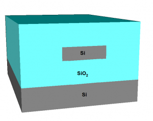
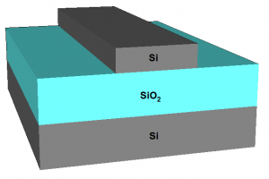
If the silicon devices require isolation from the outside environment, silicon dioxide can be deposited onto the device using a chemical vapour deposition (CVD) process. Our standard oxide deposition thickness is is 2.2 µm, which is sufficient for most thermal and optical applications. The oxide deposition process can be combined with our tri-layer heater metallization process to fabricate active photonic devices that can be controlled with temperature. Custom oxide thicknesses up to 2.2 µm can be requested.
Metallization adds electrical functionality to your device. ANT has two metallization processes, which are either performed directly on the silicon features or on top of the oxide cladding (if deposited in the previous step). The former enables the direct application of a voltage/current to a silicon device, and the latter enables low-loss thermo-optic photonic devices.
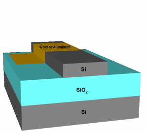
The purpose of direct metallization is to create bonding and/or probing pads and to pattern coarse electronic pathways directly on the silicon devices. This metallization process uses photolithography to define the metal areas (minimum 5 µm feature size) to within a 2 µm alignment precision to the underlying silicon layer. Metals are deposited on the substrate using electron-beam evaporation and can be controlled to an accuracy of < 1 nm. Oxide cladding cannot be deposited on the device before direct metallization is performed. The choice of materials for the pads/traces are as follows:
| Gold (with 4 nm Cr adhesion layer) |
100 nm |
| Aluminum | 200 nm |
* Protective oxide layer not shown.
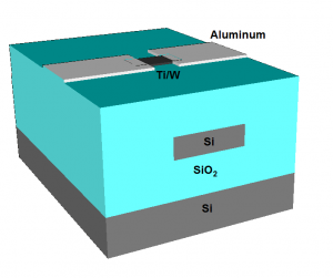
The purpose of tri-layer metallization is to create compact heater devices using a high-resistance metal and interface with the heater devices using a low-resistance routing layer. A third layer consisting of silicon dioxide is used to protect the heaters from oxidation damage. The oxide is etched away over the aluminum pads to expose them for probing or wire bonding. The use of two metals increases the electrical efficiency of the devices, as the majority of the heat generation can be targeted to a specific area of the chip with the Ti/W. The two metal layers are also patterned using photolithography . The heater layer uses a titanium-tungsten alloy to implement the high-resistance heater devices. The routing layer, which can consist of wider electrical traces or bonding/probing pads, is made out of aluminum. Below are the specifications of the tri-layer metallization process:
| Ti/W Alloy Heater Layer |
Thickness: 175 nm Bulk Resistivity: 1 μΩ-m |
| Aluminum Routing Layer |
Thickness: 500 nm Bulk Resistivity: 0.03 μΩ-m |
| Silicon Dioxide Protective Layer |
Thickness: 300 nm Bulk Resistivity: N/A |
With our deep-etch process, trenches can be made along the perimeter of the chip to allow for a fiber optic cable to couple light directly into on-chip devices such as nano-tapered waveguides and sub-wavelength gratings.
The 300 μm-wide trench is patterned around an 8.78×8.78 mm enclosed area, centered on the submitted GDSII design. A deep-etch process is then used to etch through the cladding and buffer oxide, and through the underlying silicon substrate. A final dicing process is then used to remove the edge pieces, yielding a ~9×9 mm substrate with a smooth interface on all four sides for fiber edge-coupling.
Applied Nanotools provides a set of design rules that will yield a high device manufacturing yield (> 95%). Applied Nanotools does not guarantee the optical, electrical, thermal or mechanical functionality or performance of devices that are fabricated with our service. However, we can provide metrology and optical/thermal/electrical measurement data from internal tests and from past users who have provided us with feedback.
The silicon layer is written using electron beam lithography (EBL). Unlike photolithography, EBL is a method that is susceptible to proximity effects. Although we normally correct exposures for proximity effects, extreme cases such as large areas/pads (> 10×10 µm) in close proximity to high-resolution features are difficult to correct for. Please inquire with us if your design has large areas to be exposed in conjunction with high resolution features.
Maximum design region: 9.0×9.0 mm
Minimum feature size: 60 nm (≤ 50% DC*)
Minimum spacing between features: 60 nm (≤ 50% DC*)
* For regions with duty cycle (pattered area ÷ total area) larger than 50%, the minimum dimension will be larger.
The gold/aluminum pads are patterned using photolithography. A sputtering and lift-off process is then used to transfer the metal onto the patterned areas. Because the yield of the lift-off process is highly dependent on the feature geometry, it is advised not to create areas on the design where metal can potentially be “trapped” during the lift-off process.
Maximum design region: 8.0×8.0 mm
Minimum feature size: 10 µm
Minimum spacing between features: 20 µm
The Ti/W heater, Al routing layers and Oxide windows are patterned using photolithography. A sputtering and etch process is used to transfer the metal onto the patterned areas. A thin layer of oxide is then patterned on the chips and Layer 13 is used to define pads where the oxide will be etched away to expose the aluminum pads.
Minimum feature size (Ti/W, layer 11): 2 µm
Minimum spacing between features (Ti/W, layer 11): 3 µm
Minimum feature size (Al, layer 12): 5 µm
Minimum spacing between features (Al, layer 12): 10 µm
Minimum feature size (Oxide Windows, layer 13*): 10 µm
Minimum spacing between features (Oxide Windows, layer 13*): 10 µm
* Layer 13 to be placed over regions of Layer 12 that require probing.
Maximum Design Region: 8.0×8.0 mm
Alignment tolerance between Si/TiW and TiW/Al layers: < 2 µm
Minimum Via (Overlay) Area Between TiW/Al layers: 5×5 µm
Deep-etched trenches will occur along the boundary enclosing the central 8.78×8.78 mm area of the design. It is advised to extend silicon features approx. 10 µm across the deep-etch boundary to account for misalignment. The etch will occur on all four sides of the chip.
Truncated design area: 8.78×8.78 mm (overlapping features allowed)
Alignment tolerance between deep-trench and Si layer: < 5 µm
Trench depth: 100% of thickness of substrate
Final substrate size: 8.78×8.78 mm (top); 9×9 mm (base)
Submission of a design to the NanoSOI process is done online. Design files are provided to us in Calma Graphics Data System II (GDSII) format, with database units of 1 nanometre.