產品介紹
-
-
X-Ray 波帶片
高品量的X射線光學系統,具有經過驗證的分辨率、效率和可靠性、低成本,適用於ptychography、STXM、TXM和相位對比成像的軟X射線和硬X射線
產品說明
State-of-the-art sub 20 nm Fresnel zone plate (FZP) optics for X-ray focusing and microscopy applications, including phase contrast, ptychography, and general imaging in both soft and hard X-Ray regimes. Our zone plates are used in beamlines throughout the world utilizing traditional STXM (Scanning transmission X-ray microscopy), Transmission X-ray Microscope (TXM), as well as methods including ptychography and phase contrast imaging.

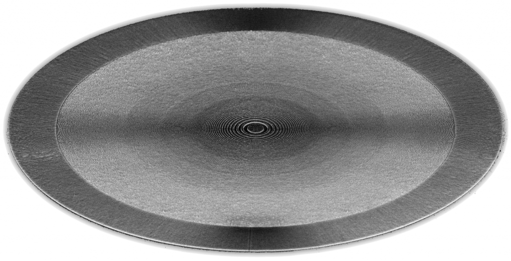
SEM Image of hard X-Ray 25 nm resolution zone plate
Advantages
High Efficiency
 |
Utilization of different metals (gold or nickel) allows for increased efficiency over a range of energies. Image generated from the ANT zone plate software. |
Soft X-Ray Specification
X-rays below 5 keV (<~0.25 nm) are typically classified as soft X-rays, where they are more readily absorbed than higher energy X-rays. Typically, zone plates do not require the same thickness for efficiency and allow for higher resolution imaging.
| Device | Outer Zone Width ΔRn(nm) | Thickness (µm) | Outer Diameter (µm) | (# of zones) E/ΔE Limit | ~ Focal Length (µm) | Estimated Lead Time |
|---|---|---|---|---|---|---|
| NZP-50um-12nm | 12 | 0.05 + 0.01 | 50 | 1059 | 144 | Please Contact |
| NZP-65um-15nm | 15 | 65 | 1096 | 235 | ||
| SZP‑90um‑15nm | 15 | <0.1 | 90 | 1514 | 325 | 2-3 |
| SZP‑120um‑15nm | 120 | 2019 | 433 | |||
| SZP‑200um‑18nm | 18 | <0.15 | 200 | 2797 | 868 | In Stock |
| SZP‑270um‑18nm | 270 | 3775 | 1172 | |||
| SZP‑320um‑18nm | 320 | 4473 | 1389 | |||
| SZP-200um-25nm | 25 | <0.24 | 200 | 2007 | 1207 | In Stock |
| SZP‑250um‑25nm | 250 | 2509 | 1510 | |||
| SZP-300um-25nm | 300 | 3010 | 1811 | |||
| SZP-360um-25nm | 360 | 3612 | 2173 | |||
| TZP‑160um‑50nm | 50 | <0.75 | 160 | 801 | 1934 | 2 – 3 |
| TZP‑280um‑50nm | 280 | 1401 | 3384 | |||
| TZP‑750um‑200nm | 200 | <0.75 | 750 | 938 | 36292 | 1 – 3 |
| TZP‑1250um‑200nm | 1250 | 1563 | 60487 | |||
| *For estimated efficiency of zone plate, please see generated graphs below or download our zone plate software. | ||||||
Hard X-Ray Specification
X-Rays above 5-10 keV transition from tender to hard X-Rays where they are better able to penetrate through samples to give better imaging. Hard X-ray Fresnel zone plates require high aspect ratio features to offer sufficient efficiency and resolution for energies above 5 keV. Our current optics give ultra-high resolution for sub 25 nm – 100 nm imaging depending on the required energy. Stacking of hard X-rays (either through double processing or chip alignment) can significantly increase the efficiency of our devices.
A range of zone plate options for hard X-Rays are available for specific requirements.
| Device | Outer Zone Width ΔRn(nm) | Thickness (µm) | Outer Diameter (µm) | (# of zones) E/ΔE Limit | Energy Range (keV) | Estimated Lead Time (months) |
|---|---|---|---|---|---|---|
| HZP-50-25nm | 25 | >0.65 | 50 | 500 | 1.5 to 10 | 2 – 3 |
| HZP-75-25nm | 75 | 750 | 2 – 3 | |||
| HZP‑100um‑42.5nm | 42.5 | >0.8 | 100 | 588 | 2 to 12 | 2 – 3 |
| HZP‑85um‑50nm | 50 | >0.9 | 85 | 425 | 2 to 12 | 2 – 3 |
| HZPX‑85um‑50nm | >1.7 | 5.5 to 20 | 4 – 6 | |||
| HZP‑180um‑50nm | >0.9 | 180 | 900 | 2 to 12 | 2 – 3 | |
| HZP‑550um‑50nm | >0.9 | 550 | 2750 | 2 to 12 | 2 – 3 | |
| HZPX‑550um‑50nm | >1.5 | 5.5 to 20 | 4 – 6 | |||
| HZP-400um-100nm | 100 | >1.2 | 400 | 1000 | 2.5 to 8 | 2 – 3 |
| HZPX‑400um‑100nm | >2.6 | 8 to 30 | 4 – 6 | |||
| HZP‑400um‑120nm | 120 | >1.5 | 400 | 834 | 5 to 25 | 2 – 3 |
| HZPX‑400um‑120nm | >2.6 | 8 to 30 | 4 – 5 | |||
| HZP‑750um‑200nm | 200 | >2.2 | 750 | 938 | 7 to 20 | 3 – 4 |
| HZPX‑750um‑200nm | 200 | >3.6 | 12 to 50 | 4 – 5 | ||
| *For estimated efficiency of zone plate, please see generated graphs below or download our zone plate software. All zone plate diameters can be customized for specific setups. Standard frame sizes are 3 mm x 3 mm with SiN membranes (100 nm). | ||||||
Central Stops
Central stop and outer blocker options significantly improve zone plate imaging, with reduction of the 0th order and improved lifetime of the optics. Various Thicknesses up to 3 µm on chip are available or >10 µm as a separate chip.

4 um thick central stop electroplated on top of Fresnel zone plate with high resolution 18 nm outer zones
Custom designs and frame sizes
Custom designs and frame sizes can be developed for specific applications. We are able to fabricate devices down to 0.1 mm and below. Our standard frame sizes are 5 mm x 5 mm and membrane thickness can be down to 50 nm while the 100 nm thickness is ideal for energies above 5 keV. We also offer silicon carbide membranes for those requiring long-lifetime membranes.

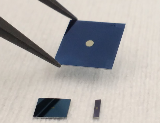
Custom silicon nitride, silicon carbide or silicon membranes down to 0.9 mm half dimensions. Image above showing 1 cm x 1 cm (top), 5 mm x 5 mm (bottom left) and 0.9 mm x 5 mm chips.
Zone Plate Calculator
Applied Nanotools offers a free online zone plate calculating theoretical efficiencies and for calculating Fresnel zone plates parameters. Please see this link to visit the webpage: Zone Plate Calculator. For the legacy software please download here (note, this version is being replaced with the new website version).


