產品介紹
-
-
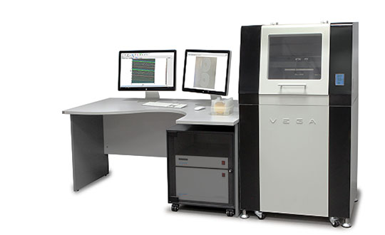
VEGA
Cutting-edge atomic force microscopy techniques for large and multiple samples
產品說明
|
|
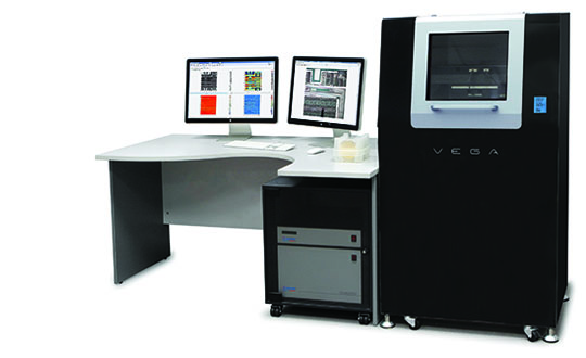 |
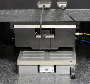
General information
|
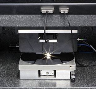
Performance
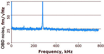
Ultimate signal-to-noise ratio of optical beam deflection (OBD) sensor
|
Most advanced set of AFM modes in basic configuration
|
||||||||||||||||||||||||||||||
產品應用
|
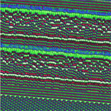
High-resolution failure analysis and roughness measurements of large and heavyweight samples |
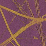
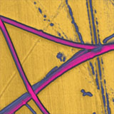
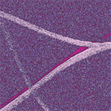
 Conventional AFM cantilever with 3:1 aspect ratio  NT-MDT wisker-type cantilever with >10:1 aspect ratio |
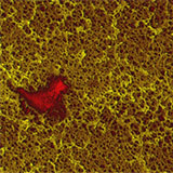 Microporous nitrocellulose membrane, obtained by NT-MDT SI Whisker type probe with 12:1 aspect ratio, 30x30 µm |
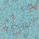
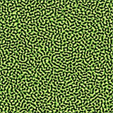
Advanced studies in a field of microelectronics, MEMS and data storage
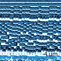
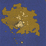
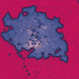
Magnetic domains
of high-density HDD |
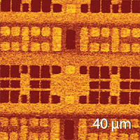
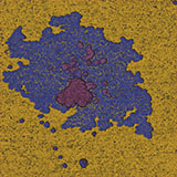
Surface potential of SRAM
|
Powerful set of surface characterization modes like Kelvin-probe, magnetic force, piezoresponce force microscopy, capacity and conductivity mapping makes VEGA AFM irreplaceable tool for research and control applications in a field of modern micro- and nanoelectronics, MEMS, NEMS and data storage. |
|
 |
|||||
|
||||||
產品規格
|
Measuring heads Scanner Scanning range, XYZ: 100×100×10 µm or 2×2×1 µm in Low Voltage Mode Closed loop: Available for all Directions: XYZ Closed loop: Available for all Directions: XYZ Drive electronics noise <5 uV/√Hz
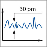
XYZ thermal drift: Down to 0.2 nm/min Moving range: 200×200 mm in XY, 30 mm in Z Positioning accuracy: 1 µm in XY, 0.2 µm in Z Positioning speed: 8 mm/sec in XY Navigation: automated multiple scanning by user-defined scenario, by video image, 3D mouse compatible Approach: smart soft approach algorithm
Optical system adjustment: automated Optical beam deflection sensor noise: <25 fm/√Hz above 50 kHz Resolution: 0,98 μm Field of view: up to 1.2×0.8 mm (5 Mpixel) Autofocus: on cantilever, on sample
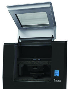
+/- 150 V voltage extender Signal access modul AFM probes: probe holder supports most of commersially available probes |
Electronics & Software Number of scan channels: virtually unlimited Signal processing: 512 Mb buffer Size, 3x 340 MHz FPGA, 320 MHz DSP Lock-in amplifiers: 2x analog lock-in amplifiers, 3x digital lock-in amplifiers (Multifrequency AFM modes supporting) Generators: 6x 32 bit digital generators, 4x for Lock-in BV: +/- 10 V AC and DC (independent sample and tip voltage supply), +/- 150 V AC and DC (optional) Self-testing: automated performance check Scanning parameters autoadjustment: drive amplitude, Automation Features: optical system adjustment, multiple Programming tools: Nova PowerScript language, LabView Database storage of obtained images PC interface: USB Instrument Isolation Acoustic isolation: build-in acoustic enclosur Seismic isolation: build-in active vibration isolation table Basic Set of Modes Contact mode: Topography, Lateral Force, Force modulation,Spreading Resistance, Multifrequency Piezo Force Microscopy,Contact Resonance Microscopy Amplitude modulation mode: Topography, Phase Imaging, Single and Double Pass Kelvin Probe Force Microscopy with Phase and Amplitude Modulation, Double Pass and Lift Magnetic Force Microscopy, Single and Double Pass Electrostatic Force Microscopy, Single and Double Pass dC/dZ and dC/dV microscopy HybriD mode: Topography, Elasticity modulus, Lift and Land Adhesion, Work of Adhesion, Current, Piezoresponse, Viscoelasticity, Force Volume Nanolithography: Voltage, Current, Force (All Vector and Raster) Spectroscopy: Force-, Amplitude-, Phase-, Frequency-, Current-Distance, I(V), Piezopulse, Custom mode Dimensions: W×L×H: 810×610×1450 mm |